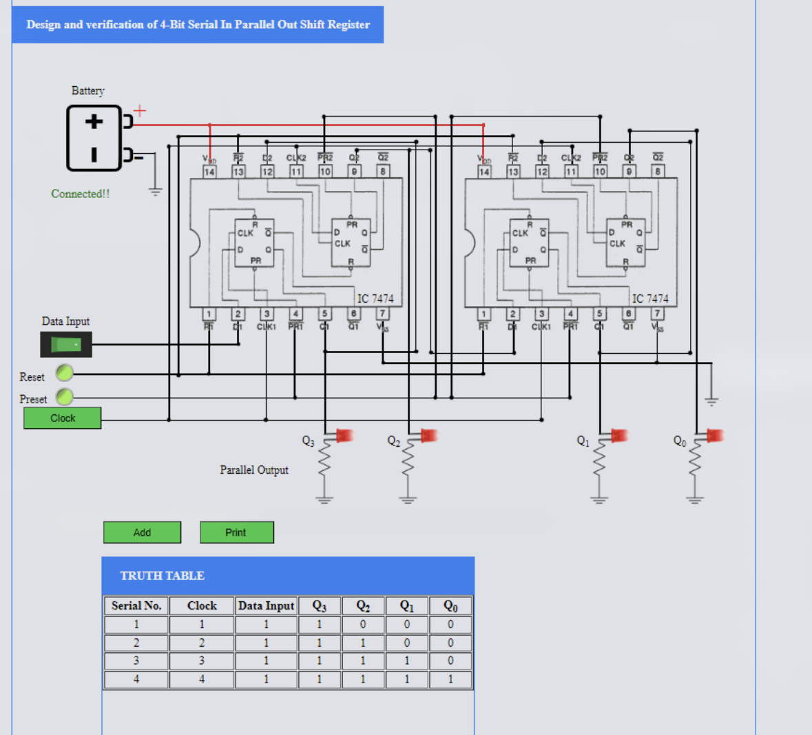
Exp 8 Design 4 bit serial in parallel out shift register
Design and Verify the 4-Bit Serial In - Parallel Out (SIPO) Shift Registers
Introduction
A Serial In - Parallel Out (SIPO) shift register is an essential component in digital electronics used for the conversion of serial data to parallel data. This shift register stores data bits serially (one after another) and then outputs them simultaneously in parallel form. It plays a crucial role in various communication systems where data needs to be processed in parallel but transmitted serially.
In this experiment, we aim to design and verify a 4-bit SIPO shift register, which will help understand the operation of how data bits are shifted serially into the register and then retrieved in parallel at the output.
Working Principle
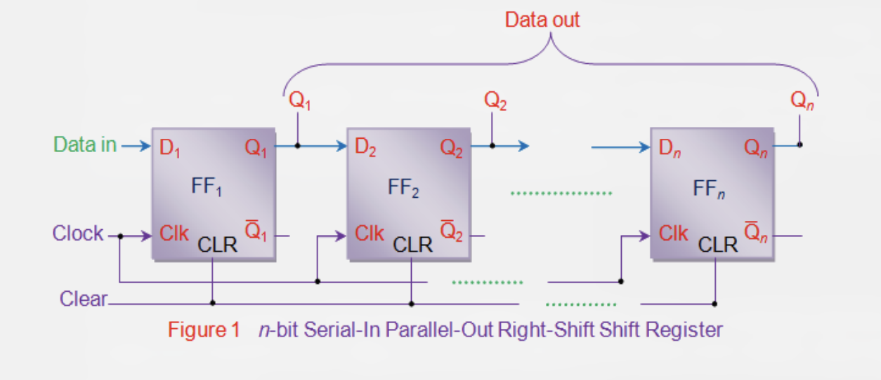
The SIPO shift register works on the principle of shifting data through flip-flops (FFs) with each clock pulse. The register comprises n flip-flops (where n is the number of bits in the data word). The input data is fed serially at the input of the first flip-flop, while the output of each flip-flop is connected to the input of the next flip-flop. This structure enables the data to be shifted from one flip-flop to the next with every rising edge of the clock signal.
- Data Input (Serial): The data word is provided bit by bit to the input of the first flip-flop (FF1).
- Clock Pulses: Each clock pulse shifts the data within the register towards the next flip-flop.
- Parallel Output: The outputs from all flip-flops (Q1, Q2, Q3, and Q4 in a 4-bit register) provide the data in parallel.
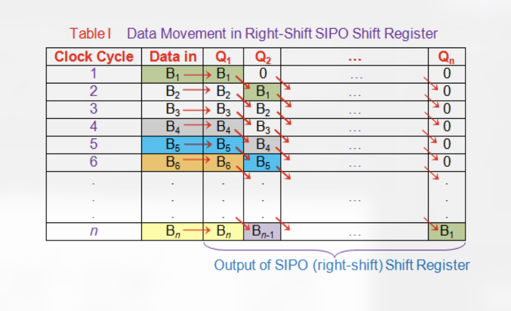
At the first clock pulse, the first bit (B1) is stored in the first flip-flop (Q1). With the second clock pulse, B1 moves to the second flip-flop (Q2), and the next bit (B2) enters FF1. This process continues for the rest of the bits in the data word. By the nth clock pulse, all the bits of the input data word will be available in parallel at the outputs of the flip-flops.
Right Shift SIPO Shift Register
In a right-shift SIPO register, the data bits shift from left to right with each clock pulse. The first bit of the input data word enters the leftmost flip-flop (FF1), and at each subsequent clock pulse, the data is shifted towards the right. The output is retrieved in parallel at the outputs of the flip-flops after the last bit has been entered.
Left Shift SIPO Shift Register
If the design is modified so that the data bits shift from right to left, we obtain a left-shift SIPO shift register. The basic working principle remains unchanged, except that the first bit (B1) is stored in the rightmost flip-flop (Q4), and subsequent bits are shifted towards the left.
Sim
Conclusion
The SIPO shift register is a fundamental component in digital electronics used to convert serial data into parallel form. Through this experiment, we understand the concept of data shifting in a register and how multiple flip-flops are used to store and retrieve bits. The design of a 4-bit SIPO shift register demonstrates the principles of serial data entry, clock pulse synchronization, and parallel data extraction.
This experiment is useful in understanding practical applications in communication systems, where data needs to be processed and transmitted in different forms (serial/parallel).