Experiment 10
Name: Tejas Sahoo
Roll No: K057
B.Tech CSE (Cybersecurity) Sem III K2
AIM
To write a VHDL code to implement the following logic gates using Vivado:
- AND gate
- OR gate
- NAND gate
- XOR gate
THEORY
VHDL
VHDL (VHSIC Hardware Description Language) is a powerful and versatile language designed for modeling, simulating, and describing digital and electronic systems. Originally developed in the 1980s for the U.S. Department of Defence under the Very High-Speed Integrated Circuits (VHSIC) program, VHDL allows engineers to define the behavior and structure of digital circuits at multiple abstraction levels—from logic gates to complex system designs. Unlike traditional programming languages, VHDL supports concurrent operations, making it essential for designing parallel-operating circuits. It is widely used in FPGA and ASIC design, enabling detailed and testable models for modern digital electronics and embedded systems.
Logic Gates
Logic gates are the basic building blocks of digital circuits, each performing a fundamental logical function on binary inputs.
- AND Gate: Outputs
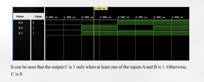
1if both inputs are1; otherwise, outputs0. - OR Gate: Outputs
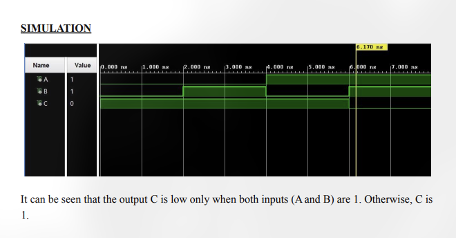
1if at least one input is1; otherwise, outputs0. - NAND Gate: Outputs
0only if both inputs are1; otherwise, outputs1. - XOR Gate: Outputs
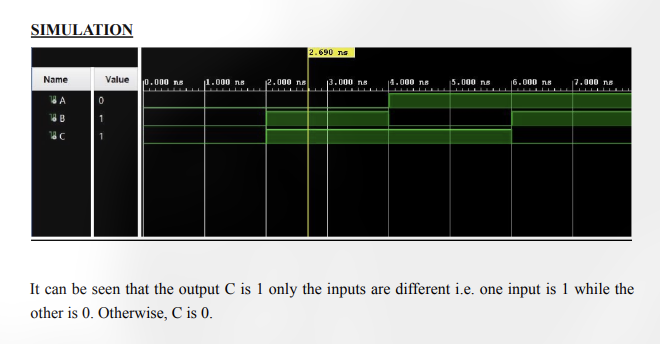
1if the inputs are different (one1and one0); otherwise, outputs0.
PROCEDURE
- Launch Vivado and create a new VHDL project.
- Write the VHDL code to define the behavior of each gate.
- Compile the VHDL code and check for syntax errors.
- Create a testbench to simulate various input combinations for each gate.
- Run the simulation in Vivado and verify the outputs against the truth table.
VHDL CODE AND SIMULATION
AND Gate
Design Source File
library IEEE;
use IEEE.STD_LOGIC_1164.ALL;

entity AND_Gate is
    Port ( A : in STD_LOGIC;
           B : in STD_LOGIC;
           C : out STD_LOGIC);
end AND_Gate;

architecture Behavioral of AND_Gate is
begin
    C <= A AND B;
end Behavioral;

---

#### **OR Gate**

**Design Source File**
```vhdl
library IEEE;
use IEEE.STD_LOGIC_1164.ALL;

entity OR_Gate is
    Port ( A : in STD_LOGIC;
           B : in STD_LOGIC;
           C : out STD_LOGIC);
end OR_Gate;

architecture Behavioral of OR_Gate is
begin
    C <= A OR B;
end Behavioral;
Simulation Source File
library IEEE;
use IEEE.STD_LOGIC_1164.ALL;

entity OR_TB is
end OR_TB;

architecture Behavioral of OR_TB is
    component OR_Gate
        port ( A : in STD_LOGIC;
               B : in STD_LOGIC;
               C : out STD_LOGIC);
    end component;

    signal A, B, C : STD_LOGIC;
begin
    dut: OR_Gate
        port map (A => A, B => B, C => C);

    stim: process
    begin
        A <= '0'; B <= '0'; wait for 2 ns;
        A <= '0'; B <= '1'; wait for 2 ns;
        A <= '1'; B <= '0'; wait for 2 ns;
        A <= '1'; B <= '1'; wait;
    end process;
end Behavioral;
NAND Gate
Design Source File
library IEEE;
use IEEE.STD_LOGIC_1164.ALL;

entity NAND_G is
    Port ( A : in STD_LOGIC;
           B : in STD_LOGIC;
           C : out STD_LOGIC);
end NAND_G;

architecture Behavioral of NAND_G is
begin
    C <= A NAND B;
end Behavioral;
Simulation Source File
library IEEE;
use IEEE.STD_LOGIC_1164.ALL;

entity NAND_TB is
end NAND_TB;

architecture Behavioral of NAND_TB is
    component NAND_G
        port ( A : in STD_LOGIC;
               B : in STD_LOGIC;
               C : out STD_LOGIC);
    end component;

    signal A, B, C : STD_LOGIC;
begin
    dut: NAND_G
        port map (A => A, B => B, C => C);

    stim: process
    begin
        A <= '0'; B <= '0'; wait for 2 ns;
        A <= '0'; B <= '1'; wait for 2 ns;
        A <= '1'; B <= '0'; wait for 2 ns;
        A <= '1'; B <= '1'; wait;
    end process;
end Behavioral;
XOR Gate
Design Source File
library IEEE;
use IEEE.STD_LOGIC_1164.ALL;

entity XOR_Gate is
    Port ( A : in STD_LOGIC;
           B : in STD_LOGIC;
           C : out STD_LOGIC);
end XOR_Gate;

architecture Behavioral of XOR_Gate is
begin
    C <= A XOR B;
end Behavioral;
Simulation Source File
library IEEE;
use IEEE.STD_LOGIC_1164.ALL;

entity XOR_TB is
end XOR_TB;

architecture Behavioral of XOR_TB is
    component XOR_Gate
        port ( A : in STD_LOGIC;
               B : in STD_LOGIC;
               C : out STD_LOGIC);
    end component;

    signal A, B, C : STD_LOGIC;
begin
    dut: XOR_Gate
        port map (A => A, B => B, C => C);

    stim: process
    begin
        A <= '0'; B <= '0'; wait for 2 ns;
        A <= '0'; B <= '1'; wait for 2 ns;
        A <= '1'; B <= '0'; wait for 2 ns;
        A <= '1'; B <= '1'; wait;
    end process;
end Behavioral;
Output
CONCLUSION
The VHDL code for implementing basic logic gates (AND Gate, OR Gate, NAND Gate, XOR Gate) was successfully written and simulated using Vivado. The truth tables of each gate were verified through the simulation results.